- 您现在的位置:买卖IC网 > Sheet目录19069 > FXO-HC335R-50 (Fox Electronics)OSCILLATOR 50.000 MHZ 3.3V SMD
FXO-HC33 Series
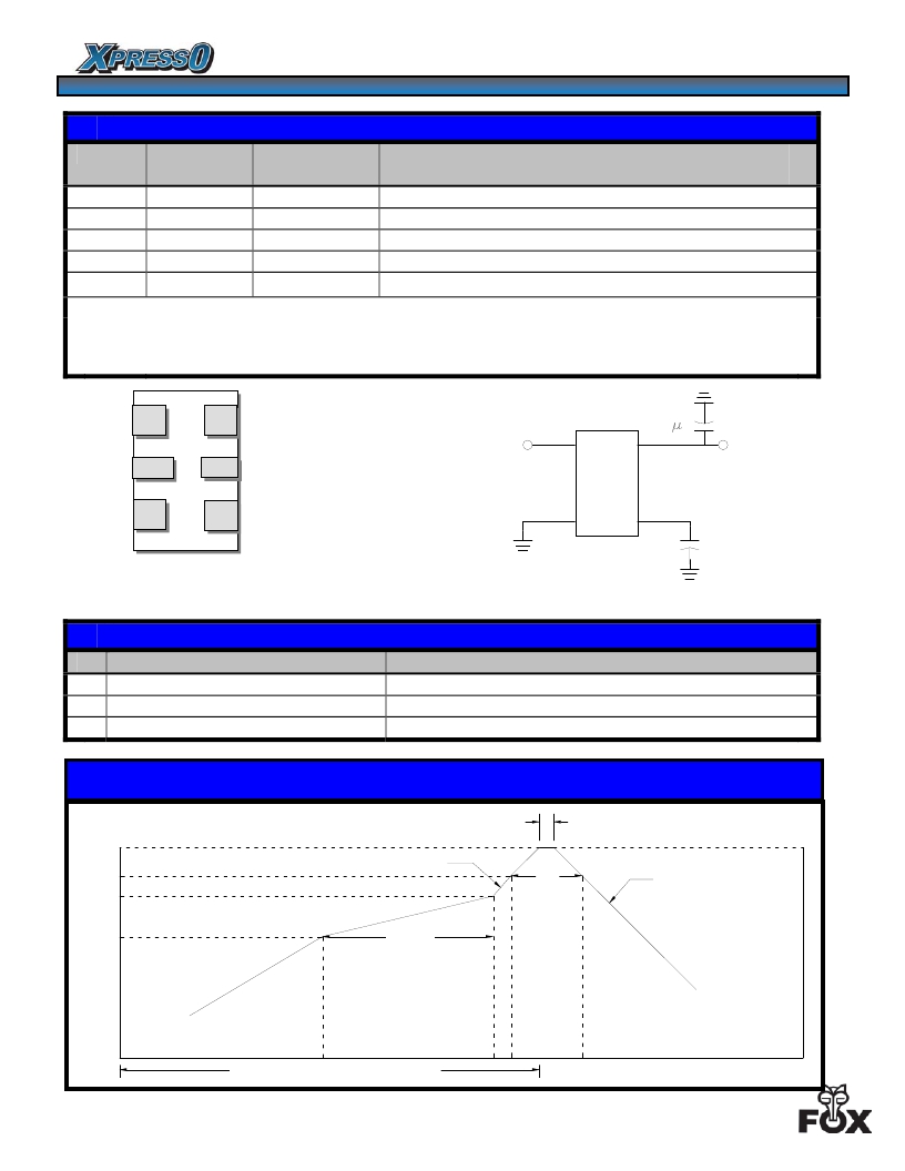
Pin Description and Recommended Circuit
Pin #
Name
Type
Function
1
E/D
1
Logic
Enable / Disable Control of Output (0 = Disabled)
2
3
GND
Output
Ground
Output
Electrical Ground for V DD
HCMOS Oscillator Output
4
V DD
2
Power
Power Supply Source Voltage
T est
P oints
N. C.
Hi Z
No Connection (Factory Use ONLY)
NOTES:
1
2
Includes pull-up resistor to V DD to provide output when the pin (1) is No Connect.
Installation should include a 0.01μF bypass capacitor placed between V DD
(Pin 4) and GND (Pin 2) to minimize power supply line noise.
E/D 1
4 V DD
0.01 F
E/D
#1
#4
V DD
N. C.
TP
TP
N. C .
NC
NC
GND 2
3 Output
GND
#2
#3
OUT
HCMOS LOAD
(15 pF)
Terminations as viewed from the Top
NOTE: X PRESS O HCMOS XOs are designed to
fit on Industry Standard, 4 pad layouts
Enable / Disable Control
Pin # 1 (state)
OPEN (No Connection)
“1” Level V IH ≥ 70% V DD
“0” Level V IL ≤ 30% V DD
Soldering Reflow Profile
Output (Pin # 3)
ACTIVE Output
ACTIVE Output
High Impedance
(2 times Maximum at 260°C for 10 seconds MAX)
t p
10 Seconds Max
within 5°C of 260°C peak
260°C
Ramp-Up
225°C
180°C
160°C
25°C
3°C/s Max
120 ± 20 Seconds
In Pre-heating Area
400 Seconds MAX from +25°C to 260°C peak
50±10 Seconds
Above 225°C Reflow Area
Ramp Down
Not to exceed 6°C/s
Page 6 of 24
? 2012 FOX ELECTRONICS | ISO9001:2008 Certified
DWG-5052
发布紧急采购,3分钟左右您将得到回复。
相关PDF资料
A0243K1
IND CTRL LED ASSY 24V RED
A0142L1
PUSHBUTTON SWITCH 16MM 6V RED
P51-15-G-P-D-5V-000-000
SENSOR 15PSI M20-1.5 6G 1-5V
LMR040-0700-27F9-10100TW
LED MOD LMR4 WM WHT 700LM 120V
A0142L2
PUSHBUTTON SWITCH 16MM 6V GREEN
LMR040-0700-27F8-10100EW
LED MOD LMR4 WM WHT 700LM 120V
P51-750-S-L-D-5V-000-000
SENSOR 750PSIS M10 5V
A0142L3
PUSHBUTTON SWITCH 16MM 6V AMBER
相关代理商/技术参数
FXO-HC335R-60-69
功能描述:标准时钟振荡器 50ppm -40 +85C 3.3V Must Specify Freq.
RoHS:否 制造商:AVX 产品:Standard Clock Oscillators 封装 / 箱体:7 mm x 5 mm 频率:75 MHz 频率稳定性:50 PPM 电源电压:2.5 V 负载电容: 端接类型:SMD/SMT 最小工作温度:0 C 最大工作温度:+ 70 C 输出格式:LVDS 尺寸: 封装:Reel 系列:
FXO-HC335R-64
功能描述:OSC 64 MHZ 3.3V HCMOS SMD RoHS:是 类别:晶体和振荡器 >> 振荡器 系列:FXO-HC33, XPRESSO 标准包装:1 系列:VG-4512CA 类型:VCXO 频率:153.6MHz 功能:三态(输出启用) 输出:LVPECL 电源电压:3.3V 频率稳定性:- 工作温度:-40°C ~ 85°C 电流 - 电源(最大):60mA 额定值:- 安装类型:表面贴装 尺寸/尺寸:0.276" L x 0.197" W(7.00mm x 5.00mm) 高度:0.071"(1.80mm) 封装/外壳:6-SMD,无引线(DFN,LCC) 包装:Digi-Reel® 电流 - 电源(禁用)(最大):- 其它名称:SER3790DKR
FXO-HC335R-66
功能描述:OSC 66 MHZ 3.3V HCMOS SMD RoHS:是 类别:晶体和振荡器 >> 振荡器 系列:FXO-HC33, XPRESSO 标准包装:1 系列:VG-4512CA 类型:VCXO 频率:153.6MHz 功能:三态(输出启用) 输出:LVPECL 电源电压:3.3V 频率稳定性:- 工作温度:-40°C ~ 85°C 电流 - 电源(最大):60mA 额定值:- 安装类型:表面贴装 尺寸/尺寸:0.276" L x 0.197" W(7.00mm x 5.00mm) 高度:0.071"(1.80mm) 封装/外壳:6-SMD,无引线(DFN,LCC) 包装:Digi-Reel® 电流 - 电源(禁用)(最大):- 其它名称:SER3790DKR
FXO-HC335R-66.66
制造商:Fox Electronics 功能描述:- Cut Tape Product 制造商:Fox Electronics 功能描述:- Tape and Reel
FXO-HC335R-66.666
功能描述:标准时钟振荡器 66MHz 3.3V 50ppm -40C to 85C
RoHS:否 制造商:AVX 产品:Standard Clock Oscillators 封装 / 箱体:7 mm x 5 mm 频率:75 MHz 频率稳定性:50 PPM 电源电压:2.5 V 负载电容: 端接类型:SMD/SMT 最小工作温度:0 C 最大工作温度:+ 70 C 输出格式:LVDS 尺寸: 封装:Reel 系列:
FXO-HC335R-7.3728
功能描述:OSC 7.3728 MHZ 3.3V HCMOS SMD RoHS:是 类别:晶体和振荡器 >> 振荡器 系列:FXO-HC33, XPRESSO 标准包装:1 系列:VG-4512CA 类型:VCXO 频率:153.6MHz 功能:三态(输出启用) 输出:LVPECL 电源电压:3.3V 频率稳定性:- 工作温度:-40°C ~ 85°C 电流 - 电源(最大):60mA 额定值:- 安装类型:表面贴装 尺寸/尺寸:0.276" L x 0.197" W(7.00mm x 5.00mm) 高度:0.071"(1.80mm) 封装/外壳:6-SMD,无引线(DFN,LCC) 包装:Digi-Reel® 电流 - 电源(禁用)(最大):- 其它名称:SER3790DKR
FXO-HC335R-70
功能描述:OSC 70 MHZ 3.3V HCMOS SMD RoHS:是 类别:晶体和振荡器 >> 振荡器 系列:FXO-HC33, XPRESSO 标准包装:1 系列:VG-4512CA 类型:VCXO 频率:153.6MHz 功能:三态(输出启用) 输出:LVPECL 电源电压:3.3V 频率稳定性:- 工作温度:-40°C ~ 85°C 电流 - 电源(最大):60mA 额定值:- 安装类型:表面贴装 尺寸/尺寸:0.276" L x 0.197" W(7.00mm x 5.00mm) 高度:0.071"(1.80mm) 封装/外壳:6-SMD,无引线(DFN,LCC) 包装:Digi-Reel® 电流 - 电源(禁用)(最大):- 其它名称:SER3790DKR
FXO-HC335R-70-79
功能描述:标准时钟振荡器 50ppm -40 +85C 3.3V Must Specify Freq.
RoHS:否 制造商:AVX 产品:Standard Clock Oscillators 封装 / 箱体:7 mm x 5 mm 频率:75 MHz 频率稳定性:50 PPM 电源电压:2.5 V 负载电容: 端接类型:SMD/SMT 最小工作温度:0 C 最大工作温度:+ 70 C 输出格式:LVDS 尺寸: 封装:Reel 系列:
